Why Choose a Laminated Bus Bar?
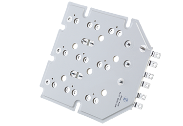
Bus bars reduce system costs, improve reliability, increase capacitance, and eliminate wiring errors. They also lower inductance and increase capacitance. Plus, the physical structure of bus bars offers unique features in mechanical design. For example, complete power distribution subsystems can also act as structural members of a total system. Multilayer bus bars offer a structural integrity that wiring methods just can’t match.
Bus Bars Reduce System Costs
A laminated bus bar will lower manufacturing costs by decreasing assembly time as well as internal material handling costs. Various conductors are terminated at customer specified locations to eliminate the guesswork usually associated with assembly operating procedures. A reduced parts count will reduce ordering, material handling and inventory costs.
Bus Bars Fabrication Allows Flexibility
Fabricated bus bars fit your specific needs and are customized for maximum efficiency.
Bus Bars Improve Reliability
Laminated bus bars can help your organization build quality into processes. The reduction of wiring errors results in fewer reworks, lower service costs and lower quality costs.
Laminated Bus Bars Increase Capacitance
Increased capacitance results in decreasing characteristic impedance. This will ultimately lead to greater effective signal suppression and noise elimination. Keeping the dielectrics thin and using dielectrics with a high relative K factor will increase capacitance.
Bus Bars Eliminate Wiring Errors
By replacing a standard cable harnesses with bus bars, the possibility for miss-wirings is eliminated. Wiring harnesses have high failure rates relative to bus bars, which have virtually none. These problems are very costly to repair. Adding bus bars to your systems is effective insurance.
Bus Bars Lower Inductance
Any conductor carrying current will develop an electromagnetic field. The use of thin parallel conductors with a thin dielectric laminated together minimizes the effect of inductance on electrical circuits. Magnetic flux cancellation is maximized when opposing potentials are laminated together. Laminated bus bars have been designed to reduce the proximity effect in many semiconductor applications as well as applications that involve high electromagnetic interference (EMI) such as SiC or GaN high frequency circuits.
Bus Bars Lower Impedance
Increasing the capacitance and reducing the inductance is a determining factor in eliminating noise. Keeping the dielectric thickness to a minimum will accomplish the highly desired low impedance.
Bus Bars Provide Denser Packaging
The use of wide, thin conductors laminated together led to decreased space requirements. Laminated bus bars have helped decrease total system size and cost.
Bus Bars Provide Wider Variety of Interconnection Methods
The flexibility of bus bars have allowed an unlimited number of interconnection styles to choose from. Bushings, embossments, and faston® tabs are most commonly used. Wire harnesses, solderable connectors, and pressed-in fittings are also integrated into the design, making a bus bar compatible with virtually any type of interface.
Bus Bars Improve Thermal Characteristics
The wide, thin conductors are favorable to allowing better airflow in systems. As package sizes decrease, the cost of removing heat from systems is greatly increased. A bus bar not only reduces the overall size of system package required, but it can also improve airflow with its sleek design.
Show lessThermal & Electrical Simulations
Temperature Rise Simulations

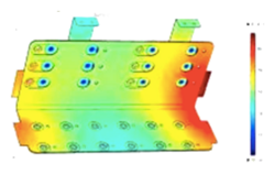
MERSEN application engineers can conduct temperature rise simulation on the bus bar prototypes. This will ensure the most thermal efficient busbar design will go to production, providing our customers optimum product performance and lowest heat dissipation. As standard practice, our design takes care of the capacitor thermal limitations by preventing it from reaching excessive overheating which in turn may dramatically affect its life-time expectancy.
Electrical Current Flow Simulations
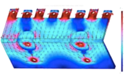
In addition to temperature rise simulations, prototype pieces can also be subjected to electrical current flow simulations. MERSEN has perfected pre-design rules over years of experience and can provide a very efficient design from the get go. Further simulation runs can in turn perfect the final design in order to provide the final product with best electrical performance.
High Frequency Skin Effect
Because of skin effect phenomena, inductance and resistance are dependent on frequency. With the emergence of high-frequency wide-bandgap technologies, currents tend to flow only on the surface of the conductor. Therefore the depth of penetration of the electromagnetic energy determines the effective conducting volume.
Semiconductor Communication Loss
When dealing with SiC, GaN or any high-speed commutation electronics applications, Mersen will achieve the lowest the lowest inductance path design to reduce semiconductor commutation losses.
Show lessIntegrated Architecture

Integrated Architecture for Power Electronics
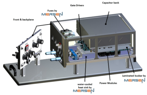
Mersen has gathered together the latest technical innovations illustrating the Integrated Architecture approach that can be offered to our inverter manufacturer clients.
Mersen’s integrated architecture approach helps inverter designers save time by optimizing the selection of key components, benefiting from a solution that is pre-designed for their specific application. Busbar, fuses, cooling, gate-drivers, capacitors, and connectors can now be optimally designed together, in one step to meet electrical, mechanical and thermal challenges of the system.
Benefits
Mersen’s power electronic bundling solution helps maximize system performance, lower total costs, and reduce time to market. Our integrated architecture comprises:
- Laminated Bus Bar:
As a superior alternative to wiring option, laminated insulated bus bar provides electrical and mechanical connection between various components. Laminated bus bar limits parasitic inductance and reduces assembly time, leading to an improvement of the overall power converter reliability, performance, and efficiency while minimizing assembly costs - Cooling Systems:
Mersen integrates its extensive cooling expertise and patented heatsink technology into semiconductor applications to make them more efficient, reliable, and profitable - Fast-acting Fuses:
Mersen Semiconductor protection fuses are used to protect against over-current conditions in power electronic equipment.
Mersen’s dedicated power electronics team is available to customize a solution for you. Make Mersen your power electronics protection partner, and you’ll discover a powerful ally that can help you protect your people and equipment. Click here for more information.
